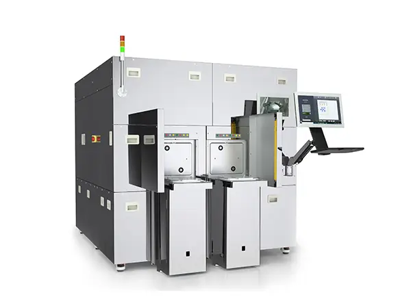
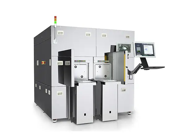
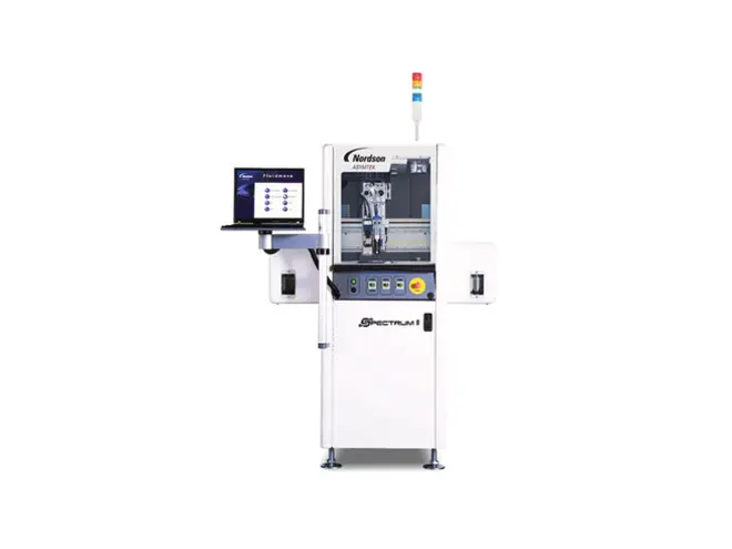
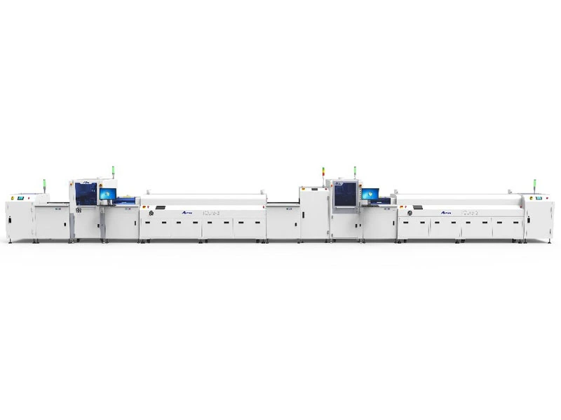
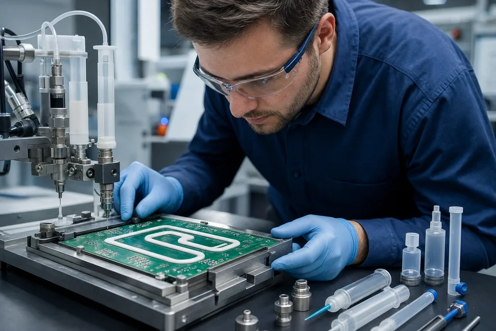
MYS Series – MYW10 Plasma System
Enabling highly flexible, high-throughput wafer surface treatment processes
With the rapid growth of the electronics assembly and semiconductor markets, industry demands for production efficiency and reliability continue to rise. By eliminating the wait times associated with traditional vacuum-based plasma processing, the MYS series cleaning equipment delivers significantly higher throughput and improved overall yields, while ensuring the safe handling of all sensitive electronic components.
CKD Technology not only has brand new machines in stock, available immediately.
We also have detailed renting business, ready to serve your specific production requirement while significantly lowering your initial investment. Contact us for more details.
CKD has a team of professional engineers, ready to deliver turn key service.
For trading of used machines, please contact us via Whatspp or email.
The MYW10 plasma system delivers a highly flexible, high-throughput wafer surface treatment process.
• Atmospheric-pressure argon plasma system
• 100mm-wide inline plasma batch processing; offers 2–5 times higher efficiency and over 30% lower operating costs compared to traditional methods
• 100% neutral plasma; safe and gentle on sensitive electronic components—no plasma bombardment, static electricity, sparks, arcing, dust, high heat, surface ripples, or UV radiation, ensuring zero damage to the product
• Versatile chemical processes: O2 process for removing organic contaminants; H2 process for removing metal oxides and activating product surfaces
• Causes no particle contamination or changes in surface roughness on the wafer
• Compatible with both wafer and tape frame production, allowing for rapid switching between the two
• Meets Class 10 cleanroom and SEMI standards
Specifications
Basic Parameters
MYW10
Power Requirements
AC 380V, 13kW, 20A, 50/60Hz
Air Pressure Requirements
90psi (6bar)
Dimensions
2000 x 2800 x 2200 mm
Weight
2200 kg
Certification Standards
SEMI S2/S6/S8
Positioning Accuracy
XY: ±20 µm @ 3σ; Z: ±10 µm @ 3σ
XYZ-Axis Repeatability
XY: ±10 µm @ 3σ; Z: ±5 µm @ 3σ
Maximum Speed
1000 mm/s (XY)
Acceleration
1.0g
Drive System
AC servo
Work Platform Specifications
Loading/Unloading Method
OHT + Load Port + Robotic Arm
Robotic Arm Payload
3 kg
Compatible Wafer Size
12-inch (300 mm)
Software Operating System
Windows 10
X/Y Travel
400 mm / 500 mm
Z-Axis Travel
20mm
Communication Protocol
SECS/GEM
Operating Range
Plasma Treatment Area (W×D)
300×300mm
Post-treatment Water Contact Angle (WCA)
WCA < 10° (Silicon wafer)
Plasma Treatment Method
O2 process for organic contaminant removal
H2 process for metal oxide removal
If you have any inquiry about a quotation or cooperation, please feel free to email or use the following inquiry form. Our sales representative will contact you within 24 hours.
We use cookies to offer you a better browsing experience, analyze site traffic and personalize content. By using this site, you agree to our use of cookies.Privacy Policy