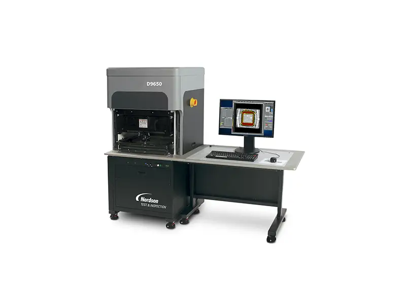
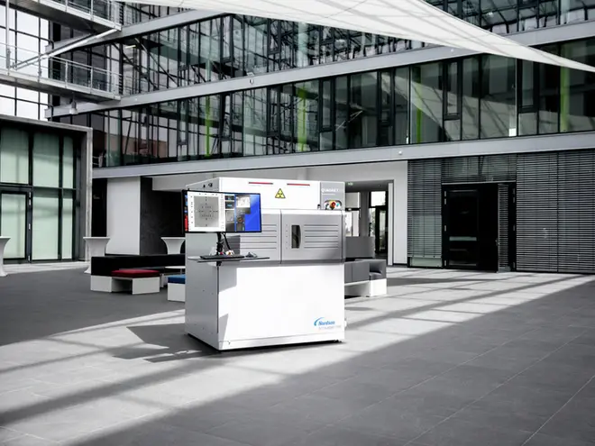
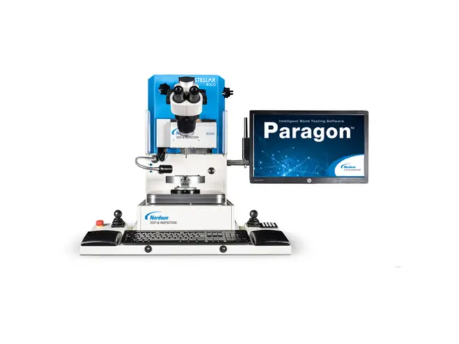
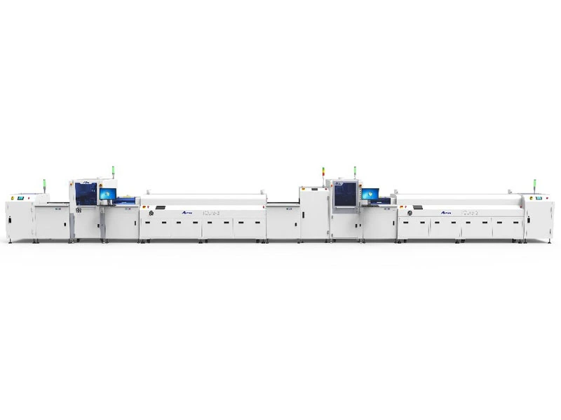
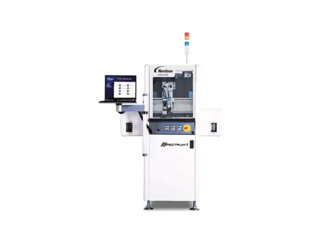
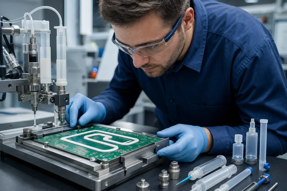
CKD provides professional Semiconductor Inspection Equipment for
microelectronics manufacturers, semiconductor assembly companies, and precision electronic
production lines. Our inspection solutions are designed to help customers identify defects,
improve process control, and maintain consistent quality throughout semiconductor packaging
and electronic manufacturing processes.
With increasing demands for miniaturized components, high-density integration, and advanced
packaging technologies, accurate inspection has become essential for improving production
reliability and reducing manufacturing risks.
Supporting Quality Control in Semiconductor Manufacturing
Modern semiconductor production requires precise inspection at different stages of the
manufacturing process. CKD supplies inspection equipment suitable for monitoring critical
parameters and detecting potential quality issues during assembly and packaging operations.
-
Surface defect inspection
-
Component alignment verification
-
Microstructure and packaging inspection
-
Assembly quality monitoring
-
Process accuracy evaluation
These inspection solutions help manufacturers improve production visibility, reduce defective
products, and optimize process stability in high-precision manufacturing environments.
Inspection Solutions for Semiconductor Packaging & Electronics
CKD provides Semiconductor Inspection Equipment for a wide range of applications, including:
-
Wafer-level packaging (WLP) inspection
-
Die attach process inspection
-
Underfill and encapsulation quality checking
-
Camera module assembly inspection
-
Microelectronic component inspection
-
Precision electronic assembly testing
By supporting different inspection requirements, CKD helps customers improve manufacturing
accuracy and achieve more reliable production outcomes.
Advanced Inspection Technologies for Higher Production Reliability
CKD supplies inspection solutions based on advanced imaging, measurement, and automation
technologies to meet the requirements of modern semiconductor production.
-
High-resolution optical inspection
-
Automated visual inspection systems
-
Precision measurement solutions
-
Intelligent inspection and analysis systems
-
Integration with automated production equipment
These technologies enable fast defect identification and provide valuable data support for
improving production efficiency and quality management.
How CKD Supports Semiconductor Inspection Applications
As an experienced Semiconductor Inspection Equipment supplier, CKD focuses
on helping customers select suitable inspection solutions according to their production
processes, accuracy requirements, and application conditions.
-
Professional equipment recommendations for different applications
-
Support for semiconductor and electronics manufacturing processes
-
Solutions adapted to different inspection requirements
-
Technical assistance during equipment selection and integration
-
Reliable supply support for global customers
Reliable Inspection Solutions for Global Semiconductor Industries
CKD works with trusted technology partners to provide Semiconductor Inspection Equipment
solutions that support advanced packaging, electronic assembly, and precision manufacturing
applications.
Whether for quality inspection, process monitoring, or production optimization, CKD helps
customers improve manufacturing control and build more reliable semiconductor production
systems.