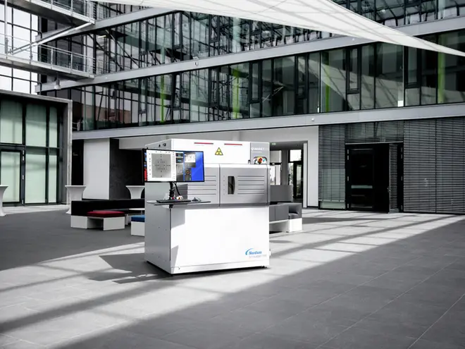
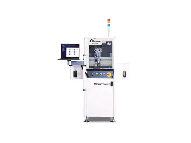
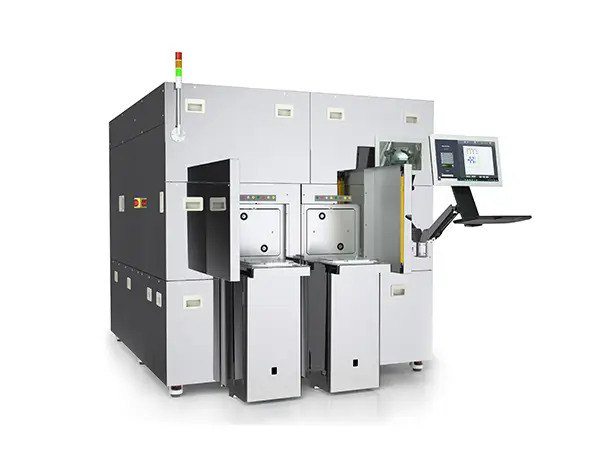
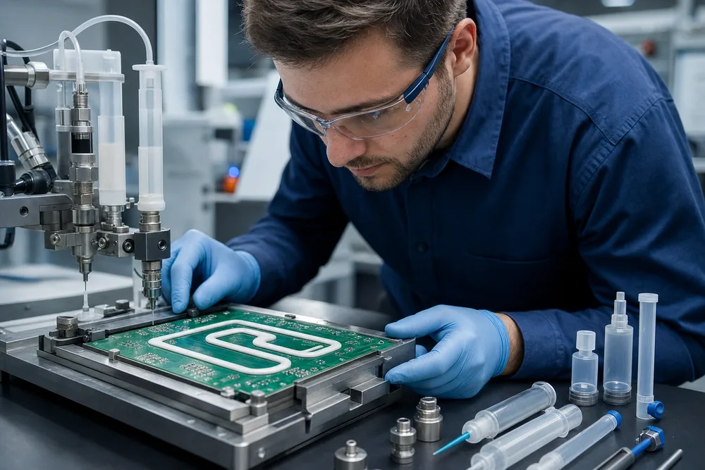
CKD provides Semiconductor X-Ray Inspection Equipment inspection solutions for semiconductor packaging,
electronics manufacturing, and precision assembly applications. These non-destructive
inspection systems help manufacturers identify hidden internal defects that cannot be
detected through conventional visual inspection methods.
As electronic components become smaller and more complex, reliable internal inspection has
become essential for improving product quality, reducing failure risks, and maintaining
stable manufacturing performance.
Detect Hidden Defects Inside Complex Assemblies
Many advanced electronic packages contain internal structures that are difficult to inspect
using traditional methods. X-Ray inspection provides clear internal imaging to help engineers
analyze assembly conditions without damaging the tested products.
-
Void detection
-
Solder joint inspection
-
Crack identification
-
Component alignment verification
-
Internal structure analysis
Advanced Inspection Capabilities for Modern Electronics
CKD supports different Semiconductor X-Ray Inspection Equipment inspection requirements according to product complexity,
inspection accuracy, and production workflow.
-
High-resolution X-Ray imaging
-
Non-destructive testing
-
Offline laboratory inspection
-
Inline automated inspection
-
Defect analysis support
These capabilities help manufacturers improve inspection efficiency while maintaining
consistent quality standards.
Applications in Semiconductor and Electronics Manufacturing
CKD Semiconductor X-Ray Inspection Equipment inspection solutions are suitable for a wide range of advanced manufacturing
applications, including:
-
Semiconductor packaging inspection
-
BGA solder joint inspection
-
Flip-chip analysis
-
PCB assembly inspection
-
Electronic component quality control
-
Automotive electronics testing
Improve Manufacturing Reliability with Internal Analysis
By revealing internal structures and potential defects, X-Ray inspection helps manufacturers
optimize production processes and improve long-term product reliability.
-
Early defect identification
-
Improved production yield
-
Reduced failure risks
-
Better process control
-
Enhanced quality assurance
Flexible X-Ray Inspection Configurations
Different industries require different inspection approaches. CKD supports customers in
selecting suitable Semiconductor X-Ray Inspection Equipment solutions based on product size, inspection requirements, and
automation objectives.
-
Inspection system selection
-
Application evaluation
-
Production line integration support
-
Inspection process optimization
-
Technical consultation
Semiconductor Inspection Support from CKD
As an experienced semiconductor inspection solution supplier, CKD provides
advanced inspection equipment and technical support for electronics manufacturers and
industrial customers.
Whether improving existing quality control processes or establishing new inspection
capabilities, CKD helps customers achieve more accurate defect analysis, higher production
reliability, and better manufacturing performance.