Inside the sterile, climate-controlled environment of a semiconductor fabrication facility, a silicon wafer embarks on a journey through hundreds of intricate processing steps. At each stage, the wafer's surface must be flawlessly clean. But after photoresist stripping, etching, or deposition, microscopic contaminants inevitably remain—organic residues, native oxides, and sub-micron particles. These invisible enemies, measuring just a few nanometers across, can cause catastrophic defects: an open circuit, a short, or a device that fails to meet performance specifications. Traditional wet cleaning methods, which rely on chemical baths and rinses, struggle to reach the bottom of high-aspect-ratio structures and can leave chemical residues that are themselves contaminants. This is the challenge that semiconductor plasma cleaning technology was created to address.
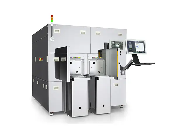
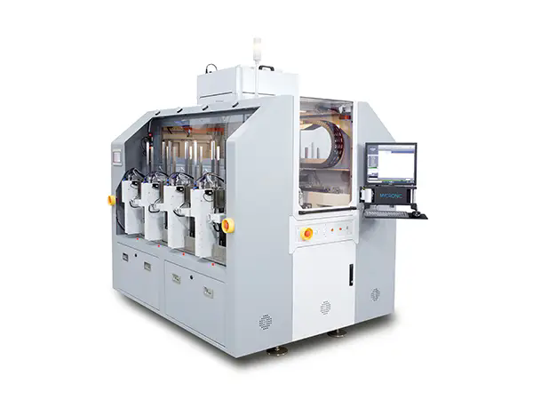
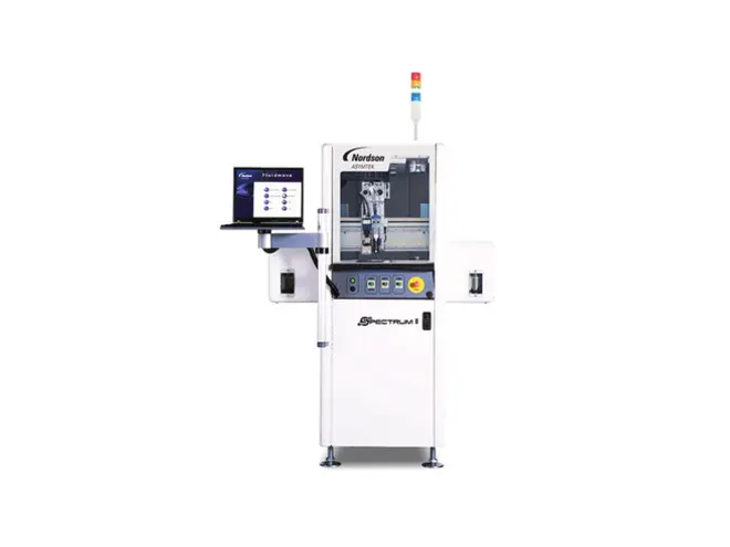
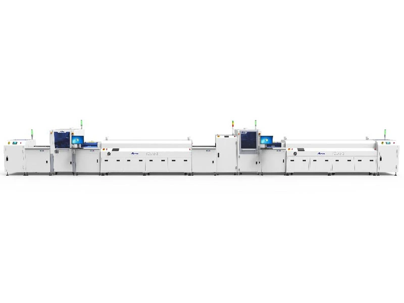
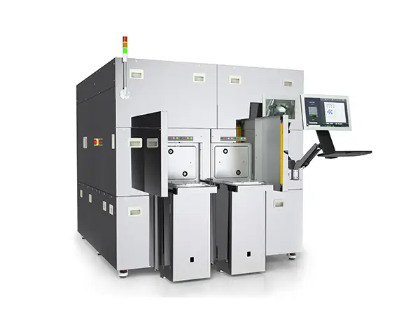
A Semiconductor Plasma Cleaner is a specialized piece of Semiconductor Inspection Equipment that uses plasma—an ionized gas containing electrons, ions, and neutral radicals—to remove contamination from semiconductor surfaces without damaging the underlying material. The process is dry, chemical-free, and highly effective at cleaning the microscopic features that characterize modern semiconductor devices. This article will provide a comprehensive technical introduction to semiconductor plasma cleaners. We will explore the fundamental physics of plasma, break down the components that make up a typical system, examine the key technical specifications that define performance, and discuss the critical role this Semiconductor Inspection Equipment plays in semiconductor manufacturing and packaging. Whether you are an engineer specifying new equipment, a technician operating these tools, or simply seeking to understand a key technology in the semiconductor supply chain, this article will provide you with the essential knowledge you need.
A Semiconductor Plasma Cleaner is a precision tool that utilizes the unique properties of plasma to clean semiconductor wafers, chip packages, lead frames, and other electronic components. At its core, the device generates an electrical discharge in a low-pressure gas, creating a highly reactive environment. This plasma—the fourth state of matter—contains a complex cocktail of highly energetic particles: ions that physically bombard the surface, free radicals that chemically react with contaminants, and electrons that help sustain the discharge. The combination of physical and chemical action effectively removes organic residues, oxides, and particulate contamination without damaging the sensitive electronic structures.
The fundamental principle behind plasma cleaning is surprisingly simple to describe, yet elegant in its execution. A process chamber is evacuated to a controlled vacuum level. A process gas—typically oxygen, argon, hydrogen, or a mixture—is introduced into the chamber. Radiofrequency (RF) or microwave power is then applied to the gas, ionizing it and creating a plasma. Within the plasma, oxygen radicals (O*) aggressively react with hydrocarbon contaminants, converting them into volatile by-products such as carbon dioxide and water vapor, which are then evacuated by the vacuum system. Simultaneously, argon ions provide a physical bombardment that helps dislodge particles and activate the surface. The result is a clean, chemically activated surface ready for the next manufacturing step.
This cleaning mechanism offers several critical advantages. The process is entirely dry, eliminating the need for liquid chemicals and the associated waste disposal. It is also inherently gentle, as the plasma temperature can be precisely controlled to avoid thermal damage. Most importantly, it is isotropic—meaning it can clean surfaces in all directions, including the insides of high-aspect-ratio features where liquid cleaning solutions cannot reach. For these reasons, the Semiconductor Plasma Cleaner has become an indispensable piece of Semiconductor Inspection Equipment in advanced semiconductor manufacturing, MEMS fabrication, and device packaging.
A modern Semiconductor Plasma Cleaner is a complex electromechanical system composed of several critical subsystems, each playing a specific role in the cleaning process. Understanding these components is essential for engineers responsible for specifying, operating, and maintaining this type of Semiconductor Inspection Equipment. The following table provides a detailed breakdown of the major components and their key characteristics.
| Component | Function | Key Selection Criteria |
| Vacuum Chamber | Encloses the processing environment and maintains vacuum conditions for plasma generation. | Material (aluminum alloy vs. stainless steel), volume, internal geometry, base pressure (typically 10^-5 Torr). |
| RF Power Supply & Matching Network | Generates and delivers the RF power (typically 13.56 MHz) to create and sustain the plasma. | Frequency (13.56 MHz is the industrial standard), power output, impedance matching capability. |
| Gas Delivery System | Controls and regulates the flow of process gases (O2, Ar, H2, CF4) into the chamber. | Mass flow controllers (MFCs), gas purity (typically 99.999% or higher), number of gas lines. |
| Vacuum Pumping System | Evacuates the chamber to the required vacuum level and removes process by-products. | Pump type (rotary vane + turbomolecular), pumping speed, ultimate vacuum level. |
| Electrode Assembly | Couples RF power into the plasma; can be capacitive or inductive coupling. | Electrode geometry (parallel plate vs. remote plasma), materials (aluminum, silicon), cooling. |
| Pressure Control System | Maintains stable process pressure through a throttle valve and pressure sensors. | Pressure sensor type (capacitance manometer, Pirani gauge), control precision, response time. |
| Control & Monitoring System | Integrates all system functions and monitors process parameters; often includes an HMI touchscreen. | Software interface, data logging, recipe management, alarm functions, connectivity (SECS/GEM for automation). |
Our factory places special emphasis on the integration and optimization of these components. The selection of the RF frequency, for instance, has profound effects on the plasma density and ion energy. While 13.56 MHz is the industry standard due to its classification as an Industrial, Scientific, and Medical (ISM) frequency band, the choice of electrode configuration determines whether the chamber operates in a direct-plasma or downstream-plasma mode. A direct-plasma (capacitively coupled) system produces a more energetic plasma suitable for physical cleaning and surface activation, while a downstream (inductively coupled) system is gentler and avoids ion damage, making it ideal for sensitive semiconductor devices.
To fully characterize a Semiconductor Plasma Cleaner, engineers must understand a set of technical specifications that define its cleaning capability, throughput, and operational envelope. These parameters directly impact the process results and should be carefully evaluated when selecting this type of Semiconductor Inspection Equipment. The table below provides a detailed overview of the critical specifications for a typical Semiconductor Plasma Cleaner system.
| Parameter | Typical Value Range | Impact on Performance |
| Chamber Volume | 20 to 200 liters | Determines batch size; larger chambers accommodate larger substrates or more wafers per run. |
| RF Power Output | 50 W to 10 kW | Higher power enables higher plasma density for faster cleaning and removal of more stubborn contaminants. |
| RF Frequency | 13.56 MHz or 2.45 GHz (microwave) | 13.56 MHz is standard; microwave (2.45 GHz) produces a more ionized plasma for specialized processes. |
| Base Pressure | 10^-5 to 10^-6 Torr | Lower base pressure reduces background contamination and improves process purity. |
| Process Pressure | 50 to 500 mTorr | Lower pressure produces more directional ion bombardment; higher pressure enhances chemical reactions. |
| Gas Flow Control | 0 to 500 sccm (standard cubic cm/min) | Precise flow control ensures reproducible gas composition and cleaning results. |
| Temperature Uniformity | +/- 5°C across the substrate | Uniform temperature ensures consistent cleaning across all parts of the substrate. |
| Uniformity of Plasma | Typically +/- 5% variation across the chamber | Good uniformity ensures that all substrates in a batch receive the same cleaning dose. |
| Cycle Time | 2 to 20 minutes (pump down to vent) | Shorter cycle time increases throughput; balance with cleaning effectiveness is key. |
These specifications are not arbitrary. For example, the base pressure of 10^-5 Torr is essential to minimize residual water vapor and oxygen in the chamber before the process gas is introduced, preventing unwanted reactions. The RF frequency of 13.56 MHz is an internationally agreed ISM frequency, selected to avoid interfering with radio communications. The gas flow control precision, typically achieved with thermal mass flow controllers, must be maintained to within +/- 1% of the set point to ensure batch-to-batch repeatability. At our factory, we maintain meticulous calibration standards and provide detailed process qualification packages with every system, ensuring our customers have the data they need to validate their processes.
Before the widespread adoption of plasma cleaning, semiconductor manufacturers relied primarily on wet chemical cleaning methods. These processes involve immersing wafers in a series of chemical baths—typically aggressive mixtures of acids and oxidizers such as "piranha" solution (sulfuric acid and hydrogen peroxide) or RCA clean (SC-1 and SC-2). While effective for many applications, wet cleaning has inherent limitations that become increasingly problematic as device dimensions shrink. As the industry moved from micron-scale to sub-100nm, the limitations of wet cleaning became critical, and plasma-based techniques emerged as a superior alternative.
Consider the experience of a major semiconductor packaging facility that was struggling with yield loss in their wire-bonding process. The assembly line was using a wet cleaning step to prepare the bond pads, but the yield remained stubbornly below 95%. The culprit was micro-contamination: residual cleaning chemicals and moisture trapped under the bond pad surface, preventing reliable gold wire attachment. After evaluating the process, the engineering team replaced the wet cleaning step with a plasma-based cleaning process. The yield immediately jumped to 99.3%, and the packaging line has maintained this performance for over three years. This is not an isolated story; it reflects a fundamental shift in the industry.
The advantages of plasma cleaning over wet cleaning are numerous and significant:
1. No Chemical Residue. Wet cleaning relies on chemicals that must be carefully rinsed away. Incomplete rinsing leaves residues that can interfere with subsequent processes, causing adhesion failures and corrosion. Plasma cleaning is a dry process that produces only volatile by-products (gases) that are pumped away, leaving no residue.
2. No Mechanical Damage. The physical agitation required in wet cleaning can cause delicate structures to collapse or detach. This is particularly critical for high-aspect-ratio features in MEMS devices and for fragile structures such as the bond pads in advanced packaging. Plasma cleaning avoids mechanical forces entirely.
3. Isotropic Cleaning Action. Wet cleaning relies on liquid chemicals that must flow into and out of surface features. The surface tension of liquids can prevent them from reaching the bottom of narrow trenches. The reactive radicals in plasma are gaseous, allowing them to penetrate and clean all exposed surfaces, regardless of feature geometry.
4. Low Process Temperature. Wet cleaning often requires elevated temperatures to achieve the required reaction rates, which can stress sensitive materials and cause thermal expansion mismatch. Plasma cleaning can be performed at near-ambient temperatures, preserving the integrity of the materials being cleaned.
5. No Hazardous Waste. The chemical by-products of wet cleaning must be treated and disposed of as hazardous waste, incurring significant environmental compliance costs. Plasma cleaning generates only gaseous by-products, which can be scrubbed using standard abatement systems.
6. Consistent, Repeatable Results. The control of plasma parameters, such as power, pressure, and gas flow, is highly accurate. A well-designed Semiconductor Plasma Cleaner produces identical conditions for every batch, removing the batch-to-batch variation that affects wet cleaning.
7. Reduced Process Steps. Wet cleaning typically requires multiple process steps: immersion in cleaning bath, rinsing, and drying. Plasma cleaning is a single-step, simple operation. This reduces equipment footprint, process time, and operator handling.
The industry's move to plasma cleaning is not just a technical preference; it is an economic and quality requirement. As semiconductor devices continue to shrink and packaging technologies become more demanding, the need for a dry, residue-free, and damage-free cleaning method will only grow. The Semiconductor Plasma Cleaner is the proven, mature technology that meets these exacting requirements.
One of the most frequent questions from engineers evaluating a Semiconductor Plasma Cleaner is: what can this equipment actually remove? The answer depends on the type of plasma and the process gas selected. Plasma cleaning can address three primary categories of contamination, each requiring a different approach and chemistry. Understanding these categories is essential for process development and equipment selection. Our factory has developed a comprehensive range of plasma cleaning solutions, with process recipes optimized for specific contamination types.
Category 1: Organic Contamination. This category includes photoresist residues, fingerprints, oils, greases, and other hydrocarbons that are introduced during semiconductor processing. These contaminants are often present as thin, invisible films that can interfere with subsequent depositions or bonding. The standard approach for organic removal is an oxygen plasma. The reactive oxygen radicals react with the carbon and hydrogen in the organic material, forming volatile carbon dioxide and water vapor that are evacuated. The plasma acts as a highly efficient, non-destructive "combustion" process at low temperature. For particularly stubborn organic residues, a mixture of oxygen with argon or hydrogen can be used to enhance the chemical reaction.
Category 2: Inorganic Contamination. This category includes native oxides (silicon dioxide, aluminum oxide), metal oxides, and other inorganic residues. These contaminants are typically removed using a reducing plasma. A common approach is a hydrogen-argon plasma, where the hydrogen radicals reduce the metal oxide back to the pure metal, effectively removing the oxide layer. Alternatively, a fluorine-based plasma (using CF4 or SF6) can be used to etch oxides, but this must be done with caution as fluorine is aggressive and can damage the underlying material. The selection of the gas mixture and the process parameters must be carefully calibrated to remove the oxide without altering the surface of the substrate. For oxides, the plasma reduces the oxide to its metallic state, removing the layer and activating the surface for adhesion.
Category 3: Particulate Contamination. This category includes microscopic dust particles, metal flakes, and other particulates that settle on the surface. These can cause defects in subsequent processes and can be sources of electrical leakage. Particulate removal is achieved through physical sputtering using an argon plasma. The argon ions strike the surface with enough energy to dislodge the particles, which are then carried away by the vacuum system. This is a purely physical cleaning process and is effective at removing particles of various sizes. However, it must be applied with appropriate energy to avoid damaging the surface or the device features.
The following table provides a more detailed mapping of contamination types to the appropriate plasma chemistry.
| Contamination Type | Common Sources | Plasma Chemistry | Cleaning Mechanism |
| Photoresist residues | Lithography, etching, stripping processes | Oxygen plasma (O2) with argon assist | Chemical oxidation: O* + CxHy → CO2 + H2O |
| Native oxide (SiO2) | Exposure to air during handling and processing | Hydrogen-argon plasma (H2/Ar) | Chemical reduction: H* + SiO2 → Si + H2O |
| Metal oxides (Al2O3, CuO) | Oxidation during processing, especially at elevated temperatures | Hydrogen plasma (H2) with argon carrier | Chemical reduction: H* + MO → M + H2O |
| Fingerprints, oils, greases | Handling by operators and storage | Oxygen plasma with fluorine clean | Chemical oxidation and volatilization |
| Particulates (dust, metal filings) | Ambient environment, wear of equipment | Argon sputtering plasma | Physical bombardment: Ar+ + particle → ejection |
| Fluorocarbon residues | Plasma etching with CF4 or SF6 gases | Oxygen plasma with Ar | Chemical oxidation of fluorocarbon film |
Our factory provides a comprehensive process development service, helping customers optimize their plasma cleaning recipes for their specific contamination challenges. We maintain a database of established processes for hundreds of substrates and contaminants, and our technical team can design customized recipes for unique applications. This ensures that your Semiconductor Plasma Cleaner delivers optimal performance for your specific manufacturing requirements.
While semiconductor plasma cleaning is essential for wafer fabrication, its impact on the packaging stage is arguably even more profound. Packaging—the process of connecting the semiconductor die to the outside world and providing mechanical and environmental protection—involves a series of critical steps: die attachment, wire bonding, encapsulation, and lead forming. Each of these steps requires clean, chemically active surfaces to ensure strong, reliable connections. Contaminants at the packaging stage are a major source of yield loss and field failures, and plasma cleaning has proven to be the most effective method to eliminate them.
To understand the impact of plasma cleaning on packaging yield, consider the wire bonding process. Wire bonding is a mature technology, but it remains the dominant method for making electrical connections between the die and the lead frame. The process uses ultrasonic energy, heat, and pressure to form a weld between a gold or copper wire and the bond pad on the die. For a reliable bond to form, the bond pad surface must be free of organic contamination, oxides, and particulates. These contaminants act as a barrier, preventing the intimate metal-to-metal contact required for a strong weld. The result is a weak bond that can fail during subsequent processing or during the life of the product.
In a typical semiconductor assembly line, a batch of die might have bond pad surfaces contaminated with residues from the dicing saw, storage, or handling. The initial wire bond yield might be 95%, meaning 5% of the bonds are weak or non-stick. This translates directly to scrap: every weak bond requires rework or results in a scrapped die. Now imagine the effect of a plasma cleaning step, applied immediately before wire bonding. The plasma removes the organic residues, reduces the native oxide, and chemically activates the bond pad surface, making it highly receptive to bonding. The yield on the plasma-cleaned batch increases to 99.5%, reducing the bond failure rate by 90%. This is not a theoretical calculation; it is a real-world result achieved by numerous packaging lines.
Other packaging processes that benefit significantly from plasma cleaning include:
The impact of plasma cleaning on packaging yield can be quantified. The following table shows typical improvements observed in packaging lines after the introduction of a plasma cleaning step in the process flow.
| Packaging Process | Yield Before Plasma Cleaning | Yield After Plasma Cleaning | Yield Improvement |
| Wire Bonding (Gold ball bond) | 94-96% | 99-99.5% | 3-5% |
| Die Attach (adhesive bond) | 92-94% | 98.5-99.5% | 4-6% |
| Underfill (void-free flow) | 88-92% | 97-98.5% | 6-8% |
| Molding (adhesion) | 90-93% | 97-98% | 4-6% |
Our Semiconductor Plasma Cleaner systems are designed with packaging applications in mind, offering features such as adjustable electrode spacing, batch processing capabilities, and integration with automated handling systems. We understand that in the high-volume environment of semiconductor packaging, reliability and repeatability are non-negotiable. Our equipment delivers the consistent performance needed to maximize yield and reduce waste.
Selecting the appropriate Semiconductor Plasma Cleaner for a specific application is a critical decision that requires a structured evaluation of technical requirements and operational constraints. The choice involves balancing factors such as cleaning effectiveness, throughput, cost, and compatibility with existing processes. A Semiconductor Plasma Cleaner is a significant capital investment, and choosing the wrong system can lead to suboptimal performance and wasted expenditure. Our factory has developed a structured selection framework to help customers navigate this process and select the system that is optimally matched to their needs.
Step 1: Define the Contaminant to be Removed. The first step is to identify the type of contamination that must be removed. Is it organic (photoresist, oil), inorganic (oxide), or particulate? Different contaminants require different plasma chemistries and process conditions. For example, an oxygen plasma is effective for organic removal, while a hydrogen plasma is required for oxide removal. The selection of the Semiconductor Plasma Cleaner must support the required gas chemistry.
Step 2: Characterize the Substrate. The substrate material and geometry are critical selection factors. What is the material? Is it silicon, gallium arsenide, or a ceramic? The material can be sensitive to certain plasma conditions. For example, some materials are susceptible to ion bombardment damage and require a "soft" plasma (downstream plasma configuration). The geometry is also important: does the substrate have fragile structures that might be damaged by physical bombardment? Does it have high-aspect-ratio features that require isotropic cleaning? The answers to these questions will determine the required electrode configuration and power density.
Step 3: Assess Throughput Requirements. How many substrates need to be cleaned per hour? This determines the required chamber size and the batch or inline configuration. For high-volume production, a larger chamber that can accommodate a batch of substrates is preferred. For research and development, a smaller chamber with rapid turnaround is more appropriate. The cycle time of the Semiconductor Plasma Cleaner (including pump-down, process, and venting) must be matched to the overall production tact time.
Step 4: Evaluate the Cleanroom Environment. The semiconductor manufacturing environment is highly controlled. The Semiconductor Plasma Cleaner must comply with cleanroom specifications, including the cleanliness class, ventilation, and electromagnetic compatibility. The equipment footprint and the available floor space must also be considered.
Step 5: Assess Gas Supply and Abatement. The Semiconductor Plasma Cleaner requires a supply of high-purity process gases and a means to abate (safely treat) the exhaust gases. The gas supply system must be capable of delivering the required gases at the correct flow rate and purity. The abatement system must be designed to handle the specific by-products generated by the plasma cleaning process (e.g., volatile organic compounds, fluorine compounds).
Step 6: Consider Automation and Integration. In a modern semiconductor manufacturing facility, the Semiconductor Plasma Cleaner is rarely a stand-alone tool. It is typically integrated into an automated production line. The system must be capable of interfacing with the factory's automation and control systems, typically through the SECS/GEM protocol (SEMI Equipment Communications Standard/Generic Equipment Model).
The following table summarizes the key decision factors and the questions that must be answered at each stage of the selection process.
| Selection Factor | Questions to Ask |
| Contamination Type | What materials need to be removed? (Organic, oxide, particles?) |
| Substrate Characteristics | What is the material? Is it fragile? Does it have high-aspect-ratio features? |
| Throughput Requirement | How many substrates per hour need to be processed? |
| Cleanroom Environment | What is the cleanroom class? What is the available floor space? |
| Gas Supply and Abatement | What process gases are required? How will the exhaust gases be abated? |
| Automation and Integration | Does the system need to integrate with factory automation (SECS/GEM)? |
Our factory's technical team is available to assist with the selection process, providing detailed technical data, process demonstration, and cost-benefit analysis. We understand that each application is unique, and we are committed to helping our customers select the Semiconductor Plasma Cleaner that provides the most effective and efficient cleaning solution for their specific needs.
Question 1: Will plasma cleaning damage the surface of my semiconductor wafers or devices?
Answer: When operated with the correct process parameters, plasma cleaning is a gentle, non-destructive process. The key factors are the RF power level, process pressure, and process gas selection. Direct plasma (capacitively coupled) systems produce a plasma with higher ion energy, which can be used for aggressive cleaning or surface activation. For sensitive materials, a downstream plasma system (where the plasma is generated remotely and the neutral radicals are transported to the wafer) can be used to avoid ion bombardment damage. We provide a comprehensive process development service to ensure that your plasma cleaning recipe does not damage the substrate.
Question 2: What is the difference between oxygen plasma and argon plasma cleaning?
Answer: Oxygen plasma cleaning relies primarily on chemical reactions. The reactive oxygen radicals oxidize organic contaminants, turning them into volatile carbon dioxide and water vapor. Argon plasma cleaning is primarily a physical process: the argon ions physically bombard the surface, dislodging particles and physically sputtering away thin layers. Oxygen plasma is ideal for removing organic residues, while argon plasma is used for surface activation and for removing particles that are not chemically bonded. Many plasma cleaning processes use a mixture of oxygen and argon to combine the chemical and physical cleaning action.
Question 3: What is the typical process cycle time for a semiconductor plasma cleaner?
Answer: The cycle time for a typical plasma cleaning process is between 5 and 20 minutes. This includes the pump-down time (to achieve vacuum), the process time (the plasma cleaning step), and the venting time (to return the chamber to atmospheric pressure). The actual cycle time depends on the chamber volume, the vacuum pump speed, and the cleaning time required. Our factory's Semiconductor Plasma Cleaner systems are designed for rapid pump-down and efficient processing, with typical cycle times of 8-12 minutes for standard batch applications.
Question 4: Can a semiconductor plasma cleaner be used for cleaning assembled devices and packages?
Answer: Yes, plasma cleaning is widely used for cleaning assembled devices and packages. This is often performed before molding or encapsulation to remove contaminants and improve adhesion. The plasma treatment can effectively clean the surfaces of the entire assembly, including the die, wire bonds, and lead frames, without causing damage to the delicate components. Care must be taken to select the correct process parameters to avoid any impact on the performance of the assembled device.
Question 5: Why is 13.56 MHz the most common RF frequency for plasma cleaning?
Answer: The frequency of 13.56 MHz is an internationally recognized Industrial, Scientific, and Medical (ISM) frequency band. This means that equipment operating at this frequency is not required to be licensed and will not interfere with radio communications. This allocation makes 13.56 MHz a practical standard for plasma processing equipment. Other ISM frequencies, such as 2.45 GHz (microwave), are also used for specialized plasma applications, but 13.56 MHz is the most widely used standard.
Shenzhen CKD Technology Co., Ltd., founded in 2010 and headquartered in the heart of China's tech innovation hub, is a premier supplier of high-end precision dispensing and semiconductor packaging equipment, including advanced Semiconductor Inspection Equipment. With a comprehensive inventory spanning multiple brands and models, and an ample stock of all types of accessories, we ensure stable, reliable, and continuous production for our customers. Our team of professional engineers delivers turnkey solutions, and our localized support in Singapore, Malaysia, Vietnam, and Thailand guarantees that you always have technical and quality assurance for your production. Guided by the core values of "precision, stability, and efficiency," CKD has provided intelligent manufacturing upgrades to hundreds of companies worldwide, winning widespread recognition and a solid reputation in the industry.
The Semiconductor Plasma Cleaner is a critical component of modern semiconductor manufacturing and packaging. By harnessing the unique properties of plasma—the fourth state of matter—it provides a dry, residue-free, and damage-free method for removing organic contamination, reducing native oxides, and cleaning surfaces. The technology is built on a foundation of precise engineering: the vacuum chamber, RF power supply, gas delivery system, and control electronics all work in concert to create a controlled plasma environment. As we have explored, the key technical specifications—base pressure, RF power, gas flow control—directly define the performance and cleaning capabilities of the system. The Semiconductor Plasma Cleaner is not merely a piece of equipment; it is the essential enabler for high-yield semiconductor manufacturing, MEMS fabrication, and advanced packaging, providing the surface cleanliness that is the prerequisite for every subsequent process step.
We invite you to learn more about how CKD can support your semiconductor manufacturing requirements. Our team of experienced engineers is ready to discuss your specific needs and to demonstrate how our Semiconductor Inspection Equipment can integrate seamlessly into your production line. Contact us for a free consultation or to schedule a demonstration at our facility. Contact Shenzhen CKD Technology Co., Ltd. today to discover our comprehensive range of semiconductor manufacturing and inspection solutions.